- 您现在的位置:买卖IC网 > Sheet目录2002 > KAD5610P-25Q72 (Intersil)IC ADC 10BIT 250MSPS DUAL 72-QFN
14
FN6810.2
September 10, 2009
Theory of Operation
Functional Description
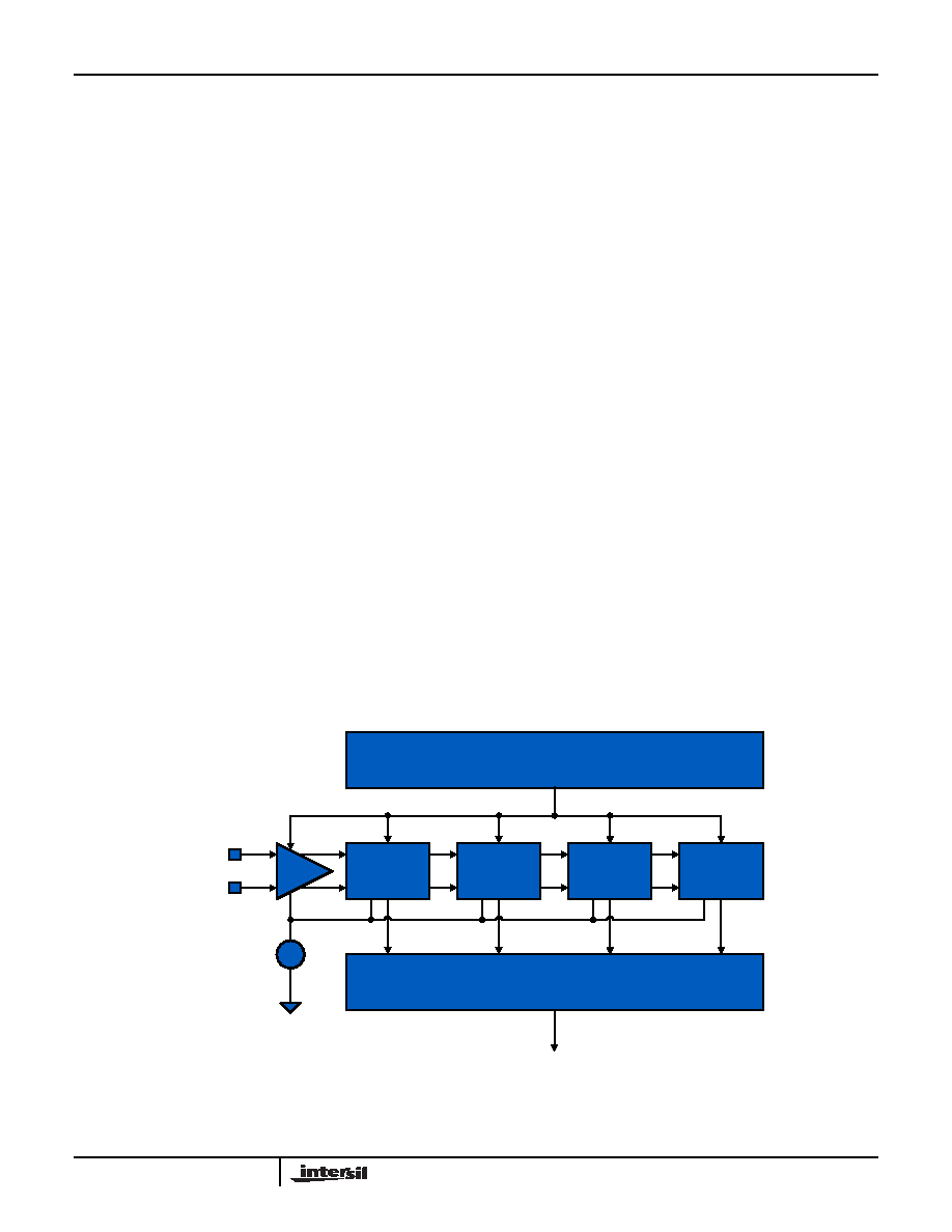
The KAD5610P is based upon a 10-bit, 250MSPS A/D
converter core that utilizes a pipelined successive
approximation architecture (Figure 22). The input voltage is
captured by a Sample-Hold Amplifier (SHA) and converted to
a unit of charge. Proprietary charge-domain techniques are
used to successively compare the input to a series of
reference charges. Decisions made during the successive
approximation operations determine the digital code for each
input value. The converter pipeline requires six samples to
produce a result. Digital error correction is also applied,
resulting in a total latency of seven and one half clock cycles.
This is evident to the user as a latency between the start of a
conversion and the data being available on the digital outputs.
The device contains two A/D converter cores with carefully
matched transfer characteristics. At start-up, each core
performs a self-calibration to minimize gain and offset errors.
The reset pin (RESETN) is initially set high at power-up and
will remain in that state until the calibration is complete. The
clock frequency should remain fixed during this time, and no
SPI communications should be attempted. Recalibration can
be initiated via the SPI port at any time after the initial
self-calibration.
Power-On Calibration
The ADC performs a self-calibration at start-up. An internal
power-on-reset (POR) circuit detects the supply voltage
ramps and initiates the calibration when the analog and
digital supply voltages are above a threshold. The following
conditions must be adhered to for the power-on calibration to
execute successfully:
A frequency-stable conversion clock must be applied to
the CLKP/CLKN pins
DNC pins (especially 3, 4 and 18) must not be pulled up or
down
SDO (pin 66) must be high
RESETN (pin 25) must begin low
SPI communications must not be attempted
A user-initiated reset can subsequently be invoked in the
event that the above conditions cannot be met at power-up.
The SDO pin requires an external 4.7k
Ω pull-up to OVDD. If
the SDO pin is pulled low externally during power-up,
calibration will not be executed properly.
After the power supply has stabilized the internal POR
releases RESETN and an internal pull-up pulls it high, which
starts the calibration sequence. If a subsequent
user-initiated reset is required, the RESETN pin should be
connected to an open-drain driver with a drive strength of
less than 0.5mA.
The calibration sequence is initiated on the rising edge of
RESETN, as shown in Figure 23. The over-range output
(OR) is set high once RESETN is pulled low, and remains in
that state until calibration is complete. The OR output returns
to normal operation at that time, so it is important that the
analog input be within the converter’s full-scale range to
observe the transition. If the input is in an over-range
condition the OR pin will stay high, and it will not be possible
to detect the end of the calibration cycle.
FIGURE 22. ADC CORE BLOCK DIAGRAM
DIGITAL
ERROR
CORRECTION
SHA
1.25V
INP
INN
CLOCK
GENERATION
2.5-BIT
FLASH
6-STAGE
1.5-BIT/STAGE
3-STAGE
1-BIT/STAGE
3-BIT
FLASH
LVDS/LVCMOS
OUTPUTS
+
–
KAD5610P
发布紧急采购,3分钟左右您将得到回复。
相关PDF资料
KAD5612P-17Q72
IC ADC 12BIT 170MSPS DUAL 72-QFN
LA72715NV-TLM-E
IC AUDIO DECODER JPN MTS 24SSOP
LICAL-DEC-LS001
IC DECODER LOW SECURITY 8DIP
LICAL-DEC-MS001
IC DECODER MS SERIES 20-SSOP
LICAL-ENC-MS001
IC ENCODER MS SERIES 20-SSOP
LICAL-TRC-MT
IC TRANSCODER MT BI-DIR 20-SSOP
LT1331CNW#PBF
IC TXRX 5V/3V RS232 28-DIP
LT1341CG#TRPBF
IC TXRX 5V RS232 SHUTDOWN 28SSOP
相关代理商/技术参数
KAD5612P
制造商:INTERSIL 制造商全称:Intersil Corporation 功能描述:Dual 12-Bit, 250/210/170/125MSPS A/D Converter
KAD5612P_09
制造商:INTERSIL 制造商全称:Intersil Corporation 功能描述:Dual 12-Bit, 250/210/170/125MSPS A/D Converter
KAD5612P_0909
制造商:INTERSIL 制造商全称:Intersil Corporation 功能描述:Dual 12-Bit, 250/210/170/125MSPS A/D Converter
KAD5612P-12Q72
功能描述:IC ADC 12BIT 125MSPS DUAL 72-QFN RoHS:是 类别:集成电路 (IC) >> 数据采集 - 模数转换器 系列:FemtoCharge™ 产品培训模块:Lead (SnPb) Finish for COTS
Obsolescence Mitigation Program 标准包装:250 系列:- 位数:12 采样率(每秒):1.8M 数据接口:并联 转换器数目:1 功率耗散(最大):1.82W 电压电源:模拟和数字 工作温度:-40°C ~ 85°C 安装类型:表面贴装 封装/外壳:48-LQFP 供应商设备封装:48-LQFP(7x7) 包装:管件 输入数目和类型:2 个单端,单极
KAD5612P-17Q72
功能描述:IC ADC 12BIT 170MSPS DUAL 72-QFN RoHS:是 类别:集成电路 (IC) >> 数据采集 - 模数转换器 系列:FemtoCharge™ 产品培训模块:Lead (SnPb) Finish for COTS
Obsolescence Mitigation Program 标准包装:250 系列:- 位数:12 采样率(每秒):1.8M 数据接口:并联 转换器数目:1 功率耗散(最大):1.82W 电压电源:模拟和数字 工作温度:-40°C ~ 85°C 安装类型:表面贴装 封装/外壳:48-LQFP 供应商设备封装:48-LQFP(7x7) 包装:管件 输入数目和类型:2 个单端,单极
KAD5612P-21Q72
制造商:Intersil Corporation 功能描述:ADC DUAL PIPELINED 210MSPS 12-BIT PARALLEL 72QFN EP - Rail/Tube 制造商:Intersil Corporation 功能描述:IC ADC 12BIT 210MSPS DUAL 72-QFN 制造商:Intersil Corporation 功能描述:12-Bit, 210MSPS Dual-Channel ADC, Programmable LVDS/LVCMOS Outputs. 72- QFN 制造商:Intersil Corporation 功能描述:KAD5612P Series Dual Ch 12-Bit SMT Analog to Digital Converter QFN-72EP 制造商:Intersil Corporation 功能描述:Analog to Digital Converters - ADC 12-BIT 210MSPS DL-CH ADC PROG LVDS/LVCMOS
KAD5612P-25Q72
制造商:Intersil Corporation 功能描述:ADC DUAL PIPELINED 250MSPS 12-BIT PARALLEL 72QFN EP - Rail/Tube 制造商:Intersil Corporation 功能描述:IC ADC 12BIT 250MSPS DUAL 72-QFN 制造商:Intersil Corporation 功能描述:IC, ADC, 12BIT, Resolution (Bits):12bit, Sampling Rate:250MSPS, Supply Voltage T
KA-D9E-011
制造商:Leach International Corporation 功能描述:MID RANGE - Bulk